
Recent progresses in microfabricating perfluorinated polymers (Teflons) and the associated new applications in microfluidics
Introduction
In the past two decades, researchers have been mining the potential of microfluidics and made substantial contributions to chemical, biological and medical research (1-3). According to George Whitesides, microfluidics is “the science and technology of systems that process or manipulate small (10−9 to 10−18 liters) amounts of fluids, using channels with dimensions of tens to hundreds of micrometers” (3). At microscale, affected by the huge increase in surface area relative to volume, the behavior of fluid is dominated by surface tension, rather than inertia (4). Therefore, the significance of surface material becomes obvious. To meet the requirements of various applications, diverse materials for microfluidics fabrication can be utilized to realize unique functions and avoid specific problems. Nowadays the most popular material in microfluidic community is polydimethylsiloxane (PDMS) because of its excellent physical properties (3,5). Nevertheless, its drawbacks can bring troubles to the researchers from various fields (5). Therefore, new materials such as hydrogel, paper, thermoplastics, and thermosets start to have their place gradually (6). Among them, perfluorinated polymers, usually known as Teflon, show an outstanding performance and great potential in both chemical and biological fields (6,7). On account of this, in this article, we focus on the whole developing progress of Teflon microfluidic chips through the discussion of their properties and corresponding applications.
Drawbacks of PDMS microfluidic chips
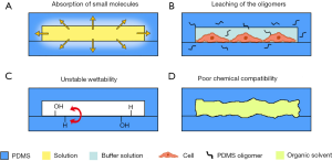
Owing to its optical transparency, flexibility, and permeability to gas, PDMS has the ability to support useful components (such as pneumatic valves and pumps), which made it the key material for exploratory research at the early stages of development. However, many studies have also shown that PDMS is not a perfect material. It has four main drawbacks, which will bring huge uncertainty in the on-chip experiments (Figure 1). A very important problem is the absorption of small molecules caused by the porous structure of PDMS (8). It is an important issue for applications in cell culture because of its impact on the concentration of soluble factors in the media, which could further affect the signaling on cell behavior and function (9,10). The second problem is the leaching of the uncrosslinked oligomers from PDMS. Cured PDMS contains residual uncrosslinked polymer chains that can freely diffuse within the bulk material. When in contact with solution, these uncrosslinked oligomers can leach out from the bulk into solution. It was found that in cell culture studies, these oligomers could incorporate into the membranes of cultured cells (10). The third problem of PDMS is the unstable surface property caused by oxygen plasma treatment. Oxygen plasma is commonly used to convert natively hydrophobic surfaces of PDMS to hydrophilic surfaces in order to facilitate chip bonding between similar or dissimilar materials. Unfortunately, its polymer chains can replace the hydroxyl groups by diffusing from the bulk to the surface and cause hydrophobic recovery (11), which raises concerns related to practicality and accessibility. Because this uncertainty could bring dynamic change to on-chip cell culture, the PDMS devices with such surface treatment must be produced within hours before the on-chip experiments, which limits the engineers’ ability to mass-produce devices beforehand. Last but not least, the chemical compatibility of PDMS, especially with organic solvents, is poor. The microchannel will swell due to PDMS’s dissolution in organic solvents and lead to changes in dimensions, integration and surface properties of the channels (12).
Liquid Teflon coating
Researchers have proposed various modification methods to break through the limitations of PDMS. However, the fabrication process turned out to be more complicated and it had not achieved superior chemical inertness or solve the other problems illustrated in Figure 1, completely (5). On the other hand, alternative materials could not replace PDMS to address the problems. Glass has been extensively used for microfluidic devices before the appearance of PDMS, but this material requires expensive facilities, hazardous chemicals and long processing time for fabrication, and it is hard to be created into certain features like valves. Some researchers also tried to develop a facile route to modify the surface of PDMS and made it more glass-like. Dong-Pyo Kim’s group grafted a preceramic polymer (allylhydridopolycarbosilane) onto the surface of PDMS channel and hydrolyzed it to form a hydrophilic coating via phase conversion. This modification gave PDMS a comparable electrokinetic performance and solvent resistance with native glass chips while maintaining optical clarity (13). However, not only the advantages of glass did it obtain, but also the shortcomings, such as brittleness that does not support pneumatic valving, and poor gas permeability that made it impossible for long-term cell culture (6). Thermoplastics such as poly(methyl methacrylate) (PMMA) and polystyrene (PS), which have also been explored for microfluidic devices, generally have similar rigidity problems with glass while still share the drawbacks in solvent compatibility that PDMS has (5). Thus, instead of improving the performance of PDMS or replacing it with other materials, an alternative way to compensate the drawbacks of PDMS is to modify its surface with a non-sticky and non-leaching material, which is also stable and has high chemical compatibility. This turns the researchers’ attention to a group of materials—fluoropolymers.
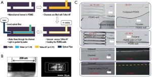
The fluoropolymer industry dates back to 1930s, beginning with the discovery of crystallized perfluoropolymers such as polytetrafluoroethylene (PTFE), which is highly chemical-resisting and thermostable but not transparent and very hard to microfabricate, and semi-crystallized perfluoropolymers such as fluorinated ethylene propylene (FEP) and perfluoroalkoxy (PFA), which are similarly inert and stable as PTFE but optically transparent and melt-processable. These solid Teflons were broadly used as coatings, films and additives, but due to the incapability in their microfabrication, they could not be used for devices in micro scale for more than half a century. Amorphous perfluoropolymers were first commercialized in 1980s to provide more flexibility in use, when Teflon AF, a copolymer of tetrafluoroethylene (TFE) and perfluoro-2,2-dimethyl-1,3-dioxole (PDD), and Cytop, a homopolymer of perfluoro-3-butenyl-vinyl ether (PBVE), were introduced by DuPont and Asahi Glass, respectively (14). Amorphous perfluoropolymers not only inherit the low surface energy, great chemical resistance, electrical properties and thermal stability of crystalline fluoropolymers, but also show higher optical transparency and lower refractive index, which extends their potential utility in coating applications in optical (15) and electrochemical (16) devices, and microfluidic channels for bioanalysis (17,18). For optical devices, Cho et al. verified that the Teflon AF coating on the optofluidic waveguide (fabricated by the method shown in Figure 2A) confined the light to the liquid core and reduced light leakage and absorption (Figure 2B) (15). For microfluidic devices, Park et al. confirmed that the Teflon AF coating on PDMS microfluidic platforms inhibited unwanted absorption of hydrophobic dye molecules (i.e., BODIPY and Nile red used to stain algae in algal lipid research) without much impact on the oxygen transfer rate and light transparency, giving a better visualization and quantification of intracellular lipid droplets in microalgae (17). In addition, Wu et al. showed that the Cytop coating on PDMS microchannels suppressed the deformation, swelling and leakage of PDMS in contact with the solvent, and prevented the adsorption of the fluorescent dye (Figure 2C) (18). Besides these extended applications, amorphous perfluoropolymers’ acceptable solvent processability also enables the processing technologies (i.e., spin-coating, dip-coating and spraying) for more special applications in ultrathin films, integrated circuits, and protective coatings (14). Thus, compared with the other perfluoropolymers, liquid Teflons are more suitable to modify the surface of PDMS and compensate for its drawbacks. However, despite these advantages of amorphous perfluoropolymers, their extremely high prices (for example, two to three times that of Teflon PFA), poor mechanical property and short lifetime restrict their use especially in an industrial scale.
Solid Teflon chip
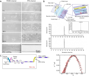
The application of liquid Teflons brought this excellent material into microfluidics community, yet this simple surface treatment could not meet the requirements of robustness and price for reliable use and mass production. On account of this, researchers started to figure out how to use solid Teflons directly to accomplish whole-Teflon chip fabrication. Like amorphous Teflons, semi-crystalline solid Teflons are extremely chemical inert, non-sticky, flexible, optically transparent, and able to prevent leaching problem, but better in hardness. These advantages are very attractive, however, the difficulty in fabrication, which was mainly caused by its high inertness, made people shrink back at the sight of it. Previous researchers have adopted materials with high melting point and mechanical strength, such as metals and silicon, as template materials, hoping that patterns on them could be transferred onto Teflon with the help of heat and pressure. Nevertheless, the transfer was unable to achieve without pattern damages. Some researchers also adopted photocurable perfluoropolyethers (PFPEs), which are a unique class of fluoropolymers that are liquids at room temperature but solidified after fully curing. This polymer exhibits low surface energy, and extremely chemically resistant like Teflon (19), which ensures its ability to fabricate microreactors for organic synthesis (20). Nevertheless, the high cost of the polymer resin limited broad applications. In 2011, we discovered that PDMS has the potential to become an ideal template material for processing Teflon (18). Based on this discovery, we developed a new molding method and gave birth to the first whole-Teflon microfluidic chip made by PFA. It showed excellent compatibility with organic solvents, outstanding non-absorbing properties, and amenability for cell culture (21). By culturing HepG2, MCF7 and HelaC3 cells in both PFA and PDMS channels, we found that the PFA surface were as cell-friendly as that of PDMS (Figure 3A), which dispelled the doubt that whether this chip could be applied to biological and medical studies. Moreover, because of Teflon’s anti-stickiness, the chips could be recyclable for cell culture experiments after simply flushing by PBS solution. We also compared the absorption ability of Teflon and PDMS by using fluorescent dyes. After washing, no fluorescence was observed in Teflon channels while the PDMS channels performed differently. This non-absorbing property brings great convenience to biomolecules fabrication as such molecules show strong adsorption or absorption in channels of other materials. Followed by this breakthrough, researches started to develop various whole-Teflon chips to realize the functions which are impossible on chips made by other materials. Zheng et al. fabricated an automated Teflon microfluidic peptide synthesizer by constructing tri-layer valves which have one PFA film between two PFA sheets (Figure 3B) (22). This microsynthesizer could generate the final decapeptide product with high quality and high through-put within 6 hours. Owing to Teflon’s outstanding chemical-inertness, fabrications using organic solvents could be carried out on microfluidic devices. Shangguan et al. generated PVA [poly (vinyl acetate)] solution droplets by using alcohol or benzene as solvent and fluorohydrocarbon with 1H,1H,2H,2H-perfluoro-1-octanol (PFO) as carrier fluid on a whole-Teflon chip, and combined it with laser light-scattering detection to realize mapping phase diagrams of polymer solutions (Figure 3C) (23).
Combination of Teflon and other materials
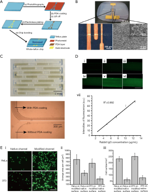
Due to the merits of Teflon materials, some devices made with other materials utilize Teflons to improve their performance such as antifouling and anti-corrosion. On the other hand, some Teflon devices are modified with other ingredients to accomplish certain functions such as hydrophilicity, electrical conductivity, and biochemical activity. On the basis of fabricating whole-Teflon microfluidic chips, the usage of solid Teflon was expanded through integration with other materials [e.g., metals (24), biomolecules (25-29), and plastics (30,31)]. Shen et al. presented a metal-Teflon hybrid, where gold electrodes were integrated onto whole-Teflon FEP chips by polydopamine (PDA)-assisted electroless plating. While the common materials for microfluidic chips are either vulnerable to organic solvents or inconvenient to fabricate, this integrated chip utilizes the unique merits of Teflon FEP, and the versatility of microfluidic techniques to enable electrochemical sensing directly in non-aqueous solvents (e.g., dichloromethane, a commonly used extractant), which offers the possibility to investigate the electrochemistry of substances that are insoluble or unstable in aqueous solutions (Figure 4A,B) (24). Another example is a biomolecule-Teflon hybrid. Teflon chips have promising applications in bioassay and cell-based experiments because of their excellent performance (i.e., anticorrosion and self-cleaning property, solvent resistance and little biomolecule adsorption). However, introducing functional groups to the chip surface is difficult due to the chemical inertness of the material. Shen et al. solved the problem by coating PDA onto whole-Teflon microfluidic chip FEP channels (Figure 4C). The PDA coating renders the Teflon surface easier for antibody immobilization in sandwich immunoassay (Figure 4D) and for cell adhesion and proliferation in cell culture (Figure 4E) (25).
Solid Teflon can also be used as coatings. Min et al. used FEP as adhesive and coatings in fabrication of multilayered polyimide (PI) film micro-reactors (30,31). They utilized the antifouling effects of superhydrophobic Teflon-FEP coating to prevent channel clogging in their 3D-flash-flow-microreactors, which enabled a long-term use or use even under challenging conditions of high polymer influx at flash flow rate of concentrated polymer, improving the production rate (30). In addition, they found that the self-adhering FEP sealed the PI layers into complex shape of the microchannel with high reproducibility and maintained the flexibility of the whole film device. Thus, they also fabricated a micro-shower flow device with FEP adhered PI micro-device and meshed membrane, which can be used to provide sufficient mixing of organic and aqueous solvent in a biphasic interfacial reaction (31). These Teflon hybrids combine the desired advantages of different materials, nevertheless, more complicated fabrication process is usually needed, compared with the fabrication of whole Teflon devices. Moreover, the lifetime of these hybrid devices is usually limited especially in harsh working environment.
Teflon stamps
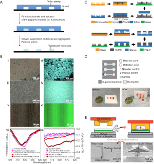
The use of microfabricated Teflon is not limited to coatings, adhesives, and microfluidic chips. Historically, perfluoropolymers have long been broadly used to assist mold release, utilizing their antisticking property; however, this was realized by coating perfluoropolymers on inorganic materials (32), which resulted in limited lifetime, especially at high working temperatures. Recently, with the capability of microfabricating Teflons, structures of micro or nano scales can be transferred to them directly, enabling fabrication of whole Teflon stamps. Compared with Teflon-inorganic hybrid stamps, the superior thermostability and acceptable thermoconductivity of whole Teflon stamps play an important role in repeatedly fabricating complementary microstructures through molding (33) and casting (34,35), as well as non-complementary microstructures through thermal deformation (36). With desired structures realized through microfabrication, Teflon materials become more competent for stamp making than other materials due to their various advantages. Shi et al. found that the Teflon stamps’ nonadsorbing property, resistance to organic solvents, and high Young’s modulus (500 MPa for Teflon and 1 MPa for PDMS) made it more reliable than conventional PDMS stamps (33). They used Teflon stamps to mold drug-laden PLGA microspheres into grooves through two routes to provide topographical cue for directing cell behavior in osteogenesis of stem cells (33). Liu et al. used Teflon stamps to cast molecules containing luminogenic silole and chiral sugar moieties into microstrips through solvent evaporation (Figure 5A), where the confined environment in the Teflon microchannels enhanced the packing order of small molecules, and thus enhanced the emission dissymmetry effect for optoelectronic applications (Figure 5B) (34). In addition, the nonstick property of the Teflon stamps rendered the adhesion force between the coating and stamp smaller than the coating and the substrate, based on which, Sun et al. made a suspending-droplet mode paper-based device (SD-µPAD) for detection of lead(II) ions (Figure 5C,D), where the channel and reservoir barriers of the device were defined by the superhydrophobic pattern generated by a Teflon contact-printing stamp (35). While Teflon’s nonstick property made the separation of stamp and product easy for large-scale production, its sufficient mechanical strength and thermoconductivity, and much higher melting point than the other plastic membranes used in fabrication enable special applications. Hu et al. designed a one-step microchannel fabrication approach through thermal deformation, using a Teflon-PFA stamp (Figure 5E), where the differences among the thermal expansion coefficient and melting point of different materials enabled the combination of generating and sealing the channel together, and therefore, a rapid production (36). Based on the excellent performance of solid Teflons in hydrophobicity, chemical inertness, mechanical strength, and nonstick property, the ability of microfabrication extends their use for stamps.
Conclusions and future prospects
In the last decade, approaches to apply perfluorinated polymers to microfluidics have evolved from coating microchannel surface with liquid Teflon to fabricating whole-Teflon chips and Teflon hybrid chips. Besides, whole-Teflon stamps have also begun to play an important role in fabricating microstructures through molding and casting. Owing to its excellent anti-fouling property, Teflon is expected to be used more broadly in the fabrication of quantitative microfluidic devices, for example, devices for studying drug-cell interaction, on-chip DNA amplification, and cell-cell communication at single-cell level. On the other hand, the solvent-resistance of Teflon microfluidic devices may lead to more applications of microfluidics in novel synthesis methods. Moreover, the unique property of microfeatured Teflon surfaces might find important new applications in self-cleaning coatings and microarray-based bioassays. Based on the outstanding reliability of Teflon materials, such products made of Teflon would be trustable in commercial applications.
Acknowledgments
The authors would like to thank Prof. Hongkai Wu from HKUST for his helpful suggestions.
Funding: This work was supported by Hong Kong Baptist University (FRG2/16-17/062, SDF 03-17-096, RC-IRMS/16-17/03), HKBU SKLEBA (SKLP_1718_P01), Hong Kong RGC (22200515), Hong Kong ITC (ITS/260/16FX), and the National Natural Science Foundation of China (21505110, 51773173).
Footnote
Conflicts of Interest: All authors have completed the ICMJE uniform disclosure form (available at http://dx.doi.org/10.21037/mps.2018.08.02). The authors have no conflicts of interest to declare.
Ethical Statement: The authors are accountable for all aspects of the work in ensuring that questions related to the accuracy or integrity of any part of the work are appropriately investigated and resolved.
Open Access Statement: This is an Open Access article distributed in accordance with the Creative Commons Attribution-NonCommercial-NoDerivs 4.0 International License (CC BY-NC-ND 4.0), which permits the non-commercial replication and distribution of the article with the strict proviso that no changes or edits are made and the original work is properly cited (including links to both the formal publication through the relevant DOI and the license). See: https://creativecommons.org/licenses/by-nc-nd/4.0/.
References
- Reyes DR, Iossifidis D, Auroux PA, et al. Micro Total Analysis Systems. 1. Introduction, Theory, and Technology. Anal Chem 2002;74:2623-36. [Crossref] [PubMed]
- Squires TM, Quake SR. Microfluidics: Fluid physics at the nanoliter scale. Rev Mod Phys 2005;77:977-1026. [Crossref]
- Whitesides GM. The origins and the future of microfluidics. Nature 2006;442:368-73. [Crossref] [PubMed]
- Atencia J, Beebe DJ. Controlled microfluidic interfaces. Nature 2005;437:648. [Crossref] [PubMed]
- Mukhopadhyay R. When PDMS isn't the best. Anal Chem 2007;79:3248-53. [Crossref] [PubMed]
- Ren K, Zhou J, Wu H. Materials for microfluidic chip fabrication. Acc Chem Res 2013;46:2396-406. [Crossref] [PubMed]
- Ren K, Chen Y, Wu H. New materials for microfluidics in biology. Curr Opin Biotechnol 2014;25:78-85. [Crossref] [PubMed]
- Toepke MW, Beebe DJ. PDMS absorption of small molecules and consequences in microfluidic applications. Lab Chip 2006;6:1484-6. [Crossref] [PubMed]
- Su X, Young EW, Underkofler HA, et al. Microfluidic cell culture and its application in high-throughput drug screening: cardiotoxicity assay for hERG channels. J Biomol Screen 2011;16:101-11. [Crossref] [PubMed]
- Regehr KJ, Domenech M, Koepsel JT, et al. Biological implications of polydimethylsiloxane-based microfluidic cell culture. Lab Chip 2009;9:2132-9. [Crossref] [PubMed]
- Eddington DT, Puccinelli JP, Beebe DJ. Thermal aging and reduced hydrophobic recovery of polydimethylsiloxane. Sens Actuators B Chem 2006;114:170-2. [Crossref]
- Lee JN, Park C, Whitesides GM. Solvent Compatibility of Poly(dimethylsiloxane)-Based Microfluidic Devices. Anal Chem 2003;75:6544-54. [Crossref] [PubMed]
- Li M, Kim DP. Silicate glass coated microchannels through a phase conversion process for glass-like electrokinetic performance. Lab Chip 2011;11:1126-31. [Crossref] [PubMed]
- Teng H. Overview of the development of the fluoropolymer industry. Appl Sci 2012;2:496-512. [Crossref]
- Cho SH, Godin J, Lo YH. Optofluidic waveguides in Teflon AF-coated PDMS microfluidic channels. IEEE Photonics Technol Lett 2009;21:1057-9. [Crossref] [PubMed]
- Yu Y, Chen J, Li J, et al. Microfabrication of a digital microfluidic platform integrated with an on-chip electrochemical cell. J Micromech Microeng 2013;23:095025 [Crossref]
- Park JW, Na S, Kang M, et al. PDMS microchannel surface modification with Teflon for algal lipid research. Biochip J 2017;11:180-6. [Crossref]
- Wu T, Suzuki H, Su Y, et al. Bio-inspired three-dimensional self-patterning of functional coatings for PDMS microfluidics. Soft Matter 2013;9:3473-7. [Crossref]
- Rolland JP, Van Dam RM, Schorzman DA, et al. Solvent-resistant photocurable “liquid teflon” for microfluidic device fabrication. J Am Chem Soc 2004;126:2322-3. [Crossref] [PubMed]
- Kim JO, Kim H, Ko DH, et al. A monolithic and flexible fluoropolymer film microreactor for organic synthesis applications. Lab Chip 2014;14:4270-6. [Crossref] [PubMed]
- Ren K, Dai W, Zhou J, et al. Whole-Teflon microfluidic chips. Proc Natl Acad Sci 2011;108:8162-6. [Crossref] [PubMed]
- Zheng H, Wang W, Li X, et al. An automated Teflon microfluidic peptide synthesizer. Lab Chip 2013;13:3347-50. [Crossref] [PubMed]
- Shangguan Y, Guo D, Feng H, et al. Mapping Phase Diagrams of Polymer Solutions by a Combination of Microfluidic Solution Droplets and Laser Light-Scattering Detection. Macromolecules 2014;47:2496-502. [Crossref]
- Shen B, Wu H. Aqueous and Nonaqueous Electrochemical Sensing on Whole-Teflon Chip. ACS Sens 2016;1:251-7. [Crossref]
- Shen B, Xiong B, Wu H. Convenient surface functionalization of whole-Teflon chips with polydopamine coating. Biomicrofluidics 2015;9:044111 [Crossref] [PubMed]
- Pivetal J, Pereira FM, Barbosa AI, et al. Covalent immobilisation of antibodies in Teflon-FEP microfluidic devices for the sensitive quantification of clinically relevant protein biomarkers. Analyst 2017;142:959-68. [Crossref] [PubMed]
- Barbosa AI, Castanheira AP, Edwards AD, et al. A lab-in-a-briefcase for rapid prostate specific antigen (PSA) screening from whole blood. Lab Chip 2014;14:2918-28. [Crossref] [PubMed]
- Reis NM, Pivetal J, Loo-Zazueta AL, et al. Lab on a stick: multi-analyte cellular assays in a microfluidic dipstick. Lab Chip 2016;16:2891-9. [Crossref] [PubMed]
- Castanheira AP, Barbosa AI, Edwards AD, et al. Multiplexed femtomolar quantitation of human cytokines in a fluoropolymer microcapillary film. Analyst 2015;140:5609-18. [Crossref] [PubMed]
- Min KI, Lee HJ, Kim DP. Three-dimensional flash flow microreactor for scale-up production of monodisperse PEG–PLGA nanoparticles. Lab Chip 2014;14:3987-92. [Crossref] [PubMed]
- Min KI, Kim JO, Kim H, et al. Multilayered film microreactors fabricated by a one-step thermal bonding technique with high reproducibility and their applications. Lab Chip 2016;16:977-83. [Crossref] [PubMed]
- Choi DG, Jeong JH, Sim YS, et al. Fluorinated Organic-Inorganic Hybrid Mold as a New Stamp for Nanoimprint and Soft Lithography. Langmuir 2005;21:9390-2. [Crossref] [PubMed]
- Shi X, Chen S, Zhou J, et al. Directing Osteogenesis of Stem Cells with Drug-Laden, Polymer-Microsphere-Based Micropatterns Generated by Teflon Microfluidic Chips. Adv Funct Mater 2012;22:3799-807. [Crossref]
- Liu J, Su H, Meng L, et al. What makes efficient circularly polarised luminescence in the condensed phase: aggregation-induced circular dichroism and light emission. Chem Sci 2012;3:2737-47. [Crossref]
- Sun H, Li W, Dong Z-Z, et al. A suspending-droplet mode paper-based microfluidic platform for low-cost, rapid, and convenient detection of lead (II) ions in liquid solution. Biosens Bioelectron 2018;99:361-7. [Crossref] [PubMed]
- Hu C, Lin S, Li W, et al. A one-step strategy for ultra-fast and low-cost mass production of plastic membrane microfluidic chips. Lab Chip 2016;16:3909-18. [Crossref] [PubMed]
Cite this article as: Wang Y, Chen S, Sun H, Li W, Hu C, Ren K. Recent progresses in microfabricating perfluorinated polymers (Teflons) and the associated new applications in microfluidics. Microphysiol Syst 2018;2:6.


